A joint South Korean and American research group has developed a scalable production method for a state of the art alloy for the use in solid state thermoelectric devices. This new alloy is nearly twice as efficient as existing materials and may lead to a new host of applications. Uses include refrigeration, consumer electronics, transportation as well as novel devices which have not been produced yet do to the inefficiencies of existing materials.
In the 1960’s, Peltier devices were primarily made from Bismuth-Telluride (Bi2Te3) or Antimony-Telluride (Sb2Te3) alloys and had a peak efficiency (zT, figure of merit) of 1.1, meaning the electricity going in was only slightly less than the heat coming out.
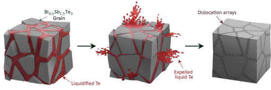
The joint team, including IBS researchers, used a process called liquid-flow assisted sintering which combined all three antimony, bismuth and telluride granules into one alloy (Bi0.5Sb1.5Te3). Additional melted tellurium was used as the liquid between the Bi0.5Sb1.5Te3 granules to help fuse them into a solid alloy, and excess Te is expelled in the process.
By creating the alloy this way, the joints between the fused grains, also known as the grain boundaries, took on a special property. Traditionally sintered Bi0.5Sb1.5Te3 have thick, coarse joints which have led to a decrease in both thermal and electrical conductivity. The new liquid-phase sintering creates grain boundaries which are organized and aligned in seams called dislocation arrays. These dislocation arrays greatly reduce their thermal conduction, leading to an enhancement of their thermoelectric conversion efficiency.
In tests, the efficiency (zT) reached 2.01 at 320 K within the range of 1.86 ±0.15 at 320 K (46.85° C) for 30 samples, nearly doubling the industry standard.
Science - Dense dislocation arrays embedded in grain boundaries for high-performance bulk thermoelectrics
Read more »


