Arxiv - Ball-grid array architecture for microfabricated ion traps
State-of-the-art microfabricated ion traps for quantum information research are approaching nearly one hundred control electrodes. We report here on the development and testing of a new architecture for microfabricated ion traps, built around ball-grid array (BGA) connections, that is suitable for increasingly complex trap designs. In the BGA trap, through-substrate vias bring electrical signals from the back side of the trap die to the surface trap structure on the top side. Gold-ball bump bonds connect the back side of the trap die to an interposer for signal routing from the carrier. Trench capacitors fabricated into the trap die replace area-intensive surface or edge capacitors. Wirebonds in the BGA architecture are moved to the interposer. These last two features allow the trap die to be reduced to only the area required to produce trapping fields. The smaller trap dimensions allow tight focusing of an addressing laser beam for fast single-qubit rotations. Performance of the BGA trap as characterized with 40Ca+ ions is comparable to previous surface-electrode traps in terms of ion heating rate, mode frequency stability, and storage lifetime. We demonstrate two-qubit entanglement operations with 171Yb+ ions in a second BGA trap.
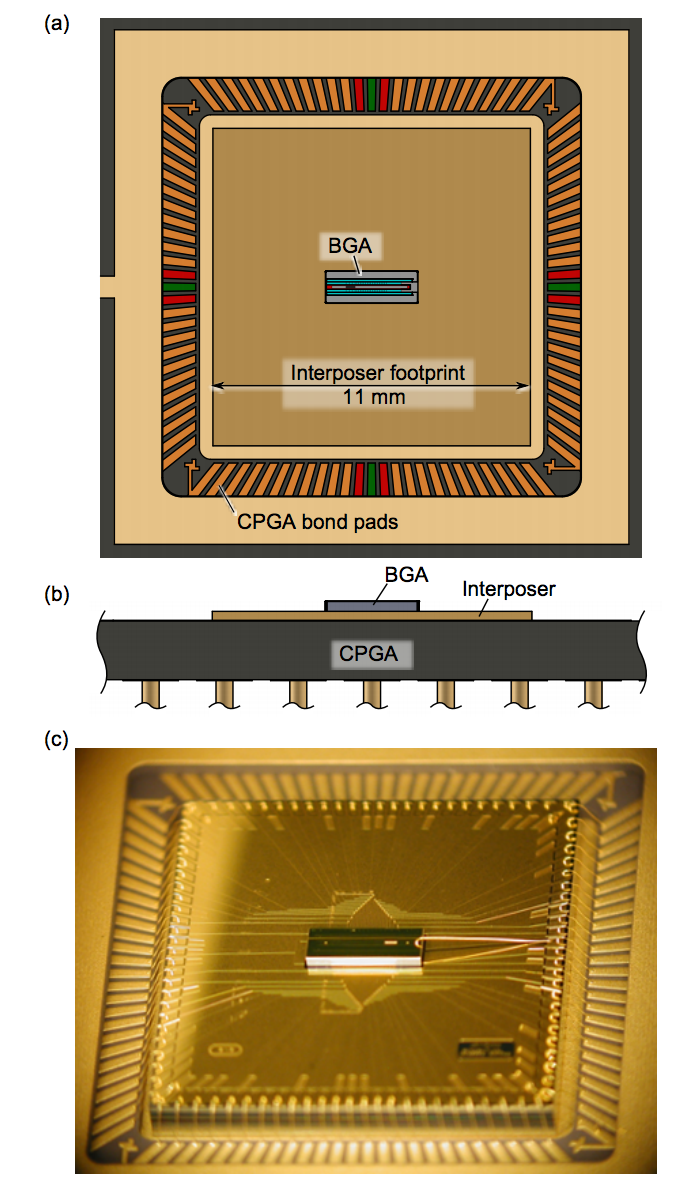
A ball-grid array architecture offers significant improvements in size and scalability for microfabricated ion traps. Trench capacitors fabricated into the trap die replace surface filter capacitors, providing a 30× reduction in trap die area over traps with planar capacitors. Through-substrate vias connect the electrodes to pads on the back side of the trap die, eliminating wirebonds from the trap surface. The trap die is bump-bonded to a separate interposer chip for signal routing to a CPGA carrier. Optical access to a trapped ion is improved by the reduced BGA trap chip area and the absence of wirebond obstructions, allowing tighter focusing of laser beams for qubit operations and addressing.
![]()
1. Overview of the BGA design: (a) Die bond region of the CPGA showing the BGA trap and the interposer footprint. (b) Side view. (c) Fully packaged BGA trap. The long bond wire supplies the trap RF signal.
Journal of Applied Physics - Ball-grid array architecture for microfabricated ion traps
Read more »![]()
![]()
![]()
![]()
![]()
![]()
![]()
![]()
![]()
![]()
![]()
State-of-the-art microfabricated ion traps for quantum information research are approaching nearly one hundred control electrodes. We report here on the development and testing of a new architecture for microfabricated ion traps, built around ball-grid array (BGA) connections, that is suitable for increasingly complex trap designs. In the BGA trap, through-substrate vias bring electrical signals from the back side of the trap die to the surface trap structure on the top side. Gold-ball bump bonds connect the back side of the trap die to an interposer for signal routing from the carrier. Trench capacitors fabricated into the trap die replace area-intensive surface or edge capacitors. Wirebonds in the BGA architecture are moved to the interposer. These last two features allow the trap die to be reduced to only the area required to produce trapping fields. The smaller trap dimensions allow tight focusing of an addressing laser beam for fast single-qubit rotations. Performance of the BGA trap as characterized with 40Ca+ ions is comparable to previous surface-electrode traps in terms of ion heating rate, mode frequency stability, and storage lifetime. We demonstrate two-qubit entanglement operations with 171Yb+ ions in a second BGA trap.
A ball-grid array architecture offers significant improvements in size and scalability for microfabricated ion traps. Trench capacitors fabricated into the trap die replace surface filter capacitors, providing a 30× reduction in trap die area over traps with planar capacitors. Through-substrate vias connect the electrodes to pads on the back side of the trap die, eliminating wirebonds from the trap surface. The trap die is bump-bonded to a separate interposer chip for signal routing to a CPGA carrier. Optical access to a trapped ion is improved by the reduced BGA trap chip area and the absence of wirebond obstructions, allowing tighter focusing of laser beams for qubit operations and addressing.
1. Overview of the BGA design: (a) Die bond region of the CPGA showing the BGA trap and the interposer footprint. (b) Side view. (c) Fully packaged BGA trap. The long bond wire supplies the trap RF signal.
Journal of Applied Physics - Ball-grid array architecture for microfabricated ion traps
Read more »


