PNAS - Nanowire nanocomputer as a finite-state machine Fundamental limits soon may end the decades-long trend in microelectronic computer circuit miniaturization that has led to much technological and economic progress. Nanoelectronic circuits using new materials, devices, and/or fabrication methods face formidable challenges to provide alternatives for future microelectronics. A key advance toward overcoming these hurdles is achieved in this work through the construction of a nanoelectronic finite-state machine (nanoFSM) computer using “bottom–up” methods. The nanoFSM integrates both computing and memory elements, which are organized from individually addressable and functionally identical nanodevices, to perform clocked, multistage logic. Furthermore, the device density is the highest reported to date for any nanoelectronic system. Advances in logic and design in the nanoFSM are scalable and should enable more extensive nanocomputers.
IEEE Spectrum summarises the work -
Researchers have arranged a total of 180 such transistor nodes in six crossbar arrays and divided them into three separate tiles to make a finite-state machine capable of performing arithmetical operations. In one configuration, the first tile does the math, while the second tile holds one bit in memory and the third tile holds a second bit. Chemist Charles Lieber, head of the Harvard team, says more tiles can be added in a Lego-like fashion. The version the team built was a two-bit adder. Four tiles would make a four-bit adder, and so on. A four-by-four array of tiles “could function as a pretty sophisticated microprocessor,” he says.
Lieber says the nanowire device will likely surpass CMOS chips only in very specific applications that benefit from low power consumption and operate at megahertz rather than gigahertz clock rates. But Ellenbogen hopes the research will provide hints for where CMOS technology can be improved. “We think some of the approaches are more generally applicable,” he says.
![]()
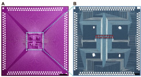
Fabricated nanoelectronic chip. (A) SEM image of the final chip (scale bar, 500 μm). (B) SEM image of the inner layout of the fabricated chip as indicated in the dashed box in A. The red dashed box region corresponds to the chip’s basic three-tile circuit shown. (Scale bar, 100 μm.) (Credit: Jun Yao et al./PNAS)
Full 10 page pdf
MITRE and Harvard have a press release on their nanowire computer.
Read more »![]()
![]()
![]()
![]()
![]()
![]()
![]()
![]()
![]()
![]()
![]()
IEEE Spectrum summarises the work -
Researchers have arranged a total of 180 such transistor nodes in six crossbar arrays and divided them into three separate tiles to make a finite-state machine capable of performing arithmetical operations. In one configuration, the first tile does the math, while the second tile holds one bit in memory and the third tile holds a second bit. Chemist Charles Lieber, head of the Harvard team, says more tiles can be added in a Lego-like fashion. The version the team built was a two-bit adder. Four tiles would make a four-bit adder, and so on. A four-by-four array of tiles “could function as a pretty sophisticated microprocessor,” he says.
Lieber says the nanowire device will likely surpass CMOS chips only in very specific applications that benefit from low power consumption and operate at megahertz rather than gigahertz clock rates. But Ellenbogen hopes the research will provide hints for where CMOS technology can be improved. “We think some of the approaches are more generally applicable,” he says.
Fabricated nanoelectronic chip. (A) SEM image of the final chip (scale bar, 500 μm). (B) SEM image of the inner layout of the fabricated chip as indicated in the dashed box in A. The red dashed box region corresponds to the chip’s basic three-tile circuit shown. (Scale bar, 100 μm.) (Credit: Jun Yao et al./PNAS)
Full 10 page pdf
MITRE and Harvard have a press release on their nanowire computer.
Read more »


